

Catalog · How the catalog works
Altium_EZ_Panelizer

- ★ 1 on GitHub
Anyone may press Interesting, signed in or not. It helps others find this project.
README
Altium EZ Panelizer
An Altium Designer script that builds a depanelisable PCB panel from a single source
.PcbDoc, by V-cut scoring or mouse bites.
Developed against Altium Designer 26.4.1 (Agile channel). DelphiScript, no SDK required.
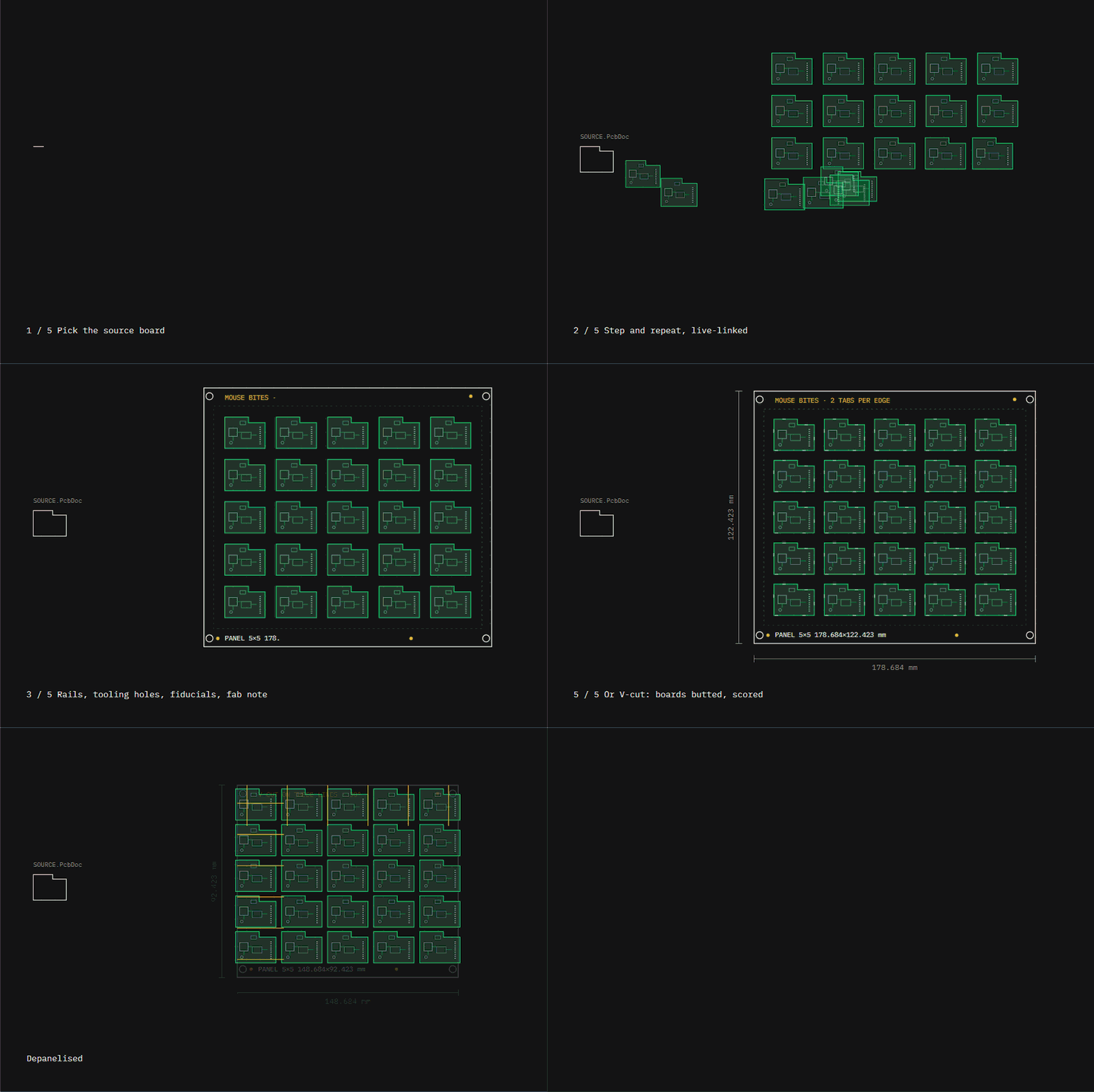
Examples
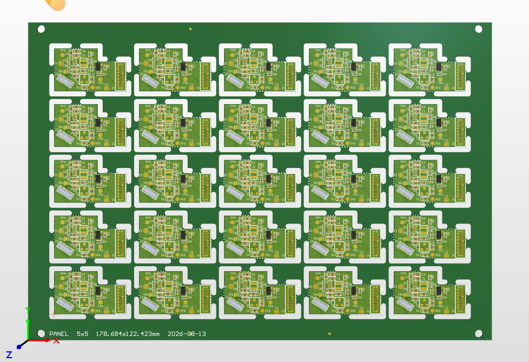
Mouse bites — 5 × 5 array, 178.684 × 122.423 mm. The router path follows each board's real outline including the notch, spliced at tabs, with the perforations sitting on the board edge.
V-cut — 5 × 5 array, 148.684 × 92.423 mm, butted boards. Score lines run clear across the panel, with rails, tooling holes, fiducials, dimensions and the fab note in the top rail.
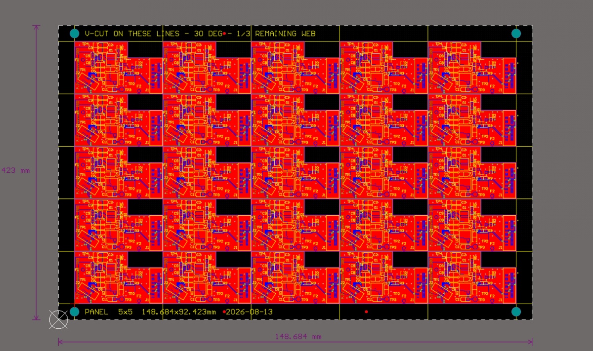
Both were generated by this script from the same source board; the panels above are the unedited output. Note the size difference for the same array — mouse-bite mode adds a routed gap between every board and around the rails, while V-cut butts them together.
What it produces
| Element | Detail |
|---|---|
| Board array | One IPCB_EmbeddedBoard, Cols x Rows, live-linked to the source PCB |
| Panel outline | Rectangular board shape sized to the array plus rails |
| Separation | V-cut score lines, or routed paths with mouse-bite tabs |
| Tooling holes | 4 NPTH in the corner rails, diameter and inset both adjustable |
| Fiducials | 3 asymmetric, 1 mm copper on the top layer |
| Title text | Panel name, array size, dimensions, date, plus a fab note for the method used |
| Dimensions | Overall width/height and array pitch, on their own mechanical layer |
| Sheet | Auto-fitted around the panel |
The panel's bottom-left corner sits on the absolute origin, so every fab coordinate is measured from that corner.
Install and run
- Open
Altium_Ez_Panelizer.PrjScrin Altium (File ▸ Open Project). - Run Script ▸
RunEzPanelizer. - Pick the source
.PcbDoc→ choose V-cut or mouse bites → set options → Build Panel.
To have it always available, add the project under Preferences ▸ Scripting System ▸ Global Projects.
If it never appears in the Run Script list, run it by process instead — this bypasses the list entirely:
Process:     ScriptingSystem:RunScriptFile
Parameters:  FileName=<path>\Altium_Ez_Panelizer.pas|ProcName=Altium_Ez_Panelizer.pas>RunEzPanelizer
The ProcName format is <file>><procedure>; the > separator is required.
Options
| Setting | Default | Notes |
|---|---|---|
| Columns / Rows | 2 x 3 | Array size |
| Gap X / Gap Y | 0 | 0 = butted. Mouse bites require a gap |
| Method | — | Asked first, on its own dialog |
| Tab width | 5.0 mm | Mouse bites only |
| Tabs per edge | 2 | Per board edge, so 8 tabs hold each board |
| Hole dia | 0.5 mm | Perforation drill size |
| Holes per tab | 5 | Count in the drill row |
| Hole pitch | 1.0 mm | Spacing between holes; row is centred in the tab |
| Hole offset | 0 | Push the row off the board edge, into the cut |
| Both sides | on | Second drill row on the far side of the cut |
| Bit | 2.0 mm | Router bit diameter |
| Rail width | 5 mm | Left/right rails optional |
| Cut layer | Mechanical 1 | Renamed and typed automatically |
| Line width | 0.2 mm | Score line width |
| Tooling hole dia | 3.0 mm | |
| Tooling hole inset | 2.5 mm | Same distance from both edges, to hole centre |
The method is chosen before the settings dialog is built, so the settings dialog only ever shows what that method uses — the whole Mouse bites group is absent under V-cut, which has no settings of its own beyond the gap and the line width.
V-cut
A V-score is a straight blade cut that runs clear across the panel, so it must follow a board edge — that is where the material has to separate.
With gap = 0 the boards are butted and each interior boundary needs one score. With a gap, that boundary gets two scores, one per adjacent board edge, and the strip between them drops out as waste. A single line down the middle of the gap would only score scrap.
Board-to-rail boundaries get one score. The panel's outer edge is never scored — it is milled.
Mouse bites
The router traces each board's actual outline — not its bounding box — so notches, steps and cutouts are followed properly. The path is spliced wherever a tab is left, and every tab is perforated along the same line so it snaps off flush with the board edge.
The path is the cutter centreline, pushed half a bit outside the outline — the cut layer is
typed Route Tool Path, so a fab routs along the line rather than compensating from it. On the
outline itself the kerf would eat half a bit into every board. Corners are solved by
intersecting the displaced edges, so convex corners extend and concave ones tuck in properly.
Perforations stay on the board edge, not the offset path, so tabs break flush.
Hole offset moves that row off the edge and into the cut, for boards carrying copper close to the outline — a 0.5 mm drill on the edge line has its own annular reach, and on a dense board that is too near the signals. It is a straight trade: whatever you offset stays on the board as a stub after the tab breaks, so keep it to what the clearance actually needs. The limit is half the bit, which is where the cutter centreline runs.
The offset applies to both rows, each measured from its own side, so a two-sided tab stays symmetric.
Both sides (default on) repeats that row on the far wall of the kerf — one full bit width off the board edge, since the centreline is half a bit out and the cut is a bit wide. A tab is held at both ends, so perforating only the board side means it snaps clean off the board and then tears off the webbing wherever it happens to give, leaving a nub on the rail or the neighbour. Two rows and both ends let go on a line.
The two rows sit one bit diameter apart, less twice the hole offset, and the hole has to be smaller than what is left or the rows meet and cut the tab through; the script checks this. It also doubles the hole count.
Two consequences worth knowing:
- A gap of at least one bit diameter is required on both axes, so the cutter fits. Below twice the bit diameter the two kerfs meet and no webbing is left between neighbouring boards — workable, but the tabs are then holding everything.
- The panel grows by one gap on each railed side. In V-cut mode the array butts straight against the rails; here the outer boards need clearance, and the material left between the cut and the rail stays behind as webbing.
Outline segments too short to hold a tab are routed solid, so the small edges of a notch do not each collect their own tabs.
Tab width and the drill row are independent. Tab width is how much material is left
un-routed; count and pitch describe the drill pattern inside it. The row is centred in the tab
and may be narrower, which usually is what you want — a little solid material at each end.
(count - 1) x pitch has to fit within the tab width, and the script checks it.
Object counts add up quickly — 6 boards x 4 edges x 2 tabs is 72 rout segments and 288 holes, or 576 with both sides perforated. Try 1 tab per edge first.
Tooling holes
Four holes, one per corner. A single inset governs both axes, so each sits on the 45° line out of its corner — the same distance down from the top as in from the side.
That distance is yours to set and is used exactly as typed. What bounds it is the rail: the hole needs half its diameter plus 0.5 mm of material on each side, so a 3 mm hole in a 5 mm rail can sit between 2.0 and 3.0 mm from the edges. Ask for more and the build stops and names the limit rather than quietly moving the holes — widen the rail and the range opens up with it.
Layers
| Layer | Name | Type |
|---|---|---|
| Cut layer (V-cut) | V-Cut |
mlVCut |
| Cut layer (mouse bites) | Routing |
mlRouteToolPath |
| Dimensions | Panel Drawing |
mlDimensions |
Dimensions deliberately go on a different mechanical layer from the cut layer. The cut layer is what the fab reads to position the blade or the router, and stray drawing lines there would be read as extra cuts.
Perforation pads are designated MB and tooling holes MH, so each group is easy to select.
Before you send it to a fab
- Tooling holes may come out plated. The
Plated := Falsecall is guarded and can be swallowed. Check the drill table. - Fiducial mask openings follow the board rule, not a forced 2 mm. Add a Mask Expansion
rule scoped to pads named
FIDif the opening is too tight. - Save the panel beside the source board so the embedded array keeps a relative link.
- Output Gerber/ODB++ from the panel. The array is a link, so the raw
.PcbDocis not self-contained.
Known limits
- Array pitch uses the source outline's bounding box. Mouse-bite rout paths follow the real outline, but arc segments are taken as the chord between their endpoints — exact for rectilinear outlines, slightly inside the true edge on a rounded corner.
- V-cut mode assumes a rectangular board, which is inherent to scoring: a straight blade cannot follow a notch. Use mouse bites for non-rectangular boards.
- Outlines longer than 512 vertices are truncated.
- The outward offset does not trim self-intersections, so a concave pocket narrower than the bit will not offset cleanly — such a pocket cannot be routed at that bit size anyway, but check it by eye rather than trusting the path.
- Dimensions are drawn from tracks and text, not
IPCB_Dimensionobjects — a drawing aid, not live measurements. Move something and the numbers will not follow. - Tabs are spaced evenly along each edge. Placing them away from connectors needs manual edits.
- Title text clears the left tooling hole only; a very long title could reach the right one.
- Vertical dimension captions sit horizontally beside the line.
License
MIT — see LICENSE. Use it, change it, ship it in commercial work; just keep the copyright notice. No warranty, which matters here: check the fab caveats above before you send a panel out.
Developer notes
NOTES.md documents the Altium DelphiScript API findings behind this script — which
properties are writable, which are read-only traps, and how to verify one without breaking
the whole unit. Worth reading before extending it.