

microwave-pcb

PCB Design project to simulate a microwave.
- Active · last change 3-11-2025
- ★ 2 on GitHub
README
microwave-pcb
PCB Design project which aims at recreating a microwave at low voltage.
Report on the work
Motivations
Over the years, I have had the opportunity to develop and deepen my knowledge in the field of mechatronics thanks to my personal investment and through internship experiences. This investment has allowed me to build a solid theoretical and practical foundation, essential for mastering complex electronic systems. My curiosity and passion for engineering have led me to diversify my projects, involving a variety of electronic devices. Today, this project of simulating the control interface of a microwave is an opportunity to demonstrate my expertise in mechatronics. This project allows me to apply the skills I have acquired over time, utilizing principles of mechatronics and embedded systems in a familiar yet complex device. Using my knowledge of programming and electronic circuit design, I have developed a solution that faithfully reproduces the functionality and ergonomics of a real microwave oven. This work illustrates my ability to tackle the technical challenges posed by electronic system design, to understand them holistically, and to propose innovative and efficient solutions. Inspiration The reproduced microwave is the MG23F301TAS model from Samsung. Its interface is simple; it has one digital clock display, two control knobs and a button. The clock both displays the hour and the cooking timer depending on the current use of the oven. The upper-most control knob selects the cooking time and rotates freely while the bottom one allows to choose the power at which the food is cooked. The bottom knob is limited to half a turn of rotation. Another feature to notice is the led that turns on when the oven door is opened to allow the user to see the turntable easily. At last, the most important element of the microwave, I decided to add a buzzer to indicate that the timer reached 0. The goal of this project is to reverse engineer this oven, while removing the power electronics of the system. As one knows, microwaves use magnetrons to emit microwaves. These magnetrons require transformers and full-bridge rectifiers to convert the usual 230 VAC (in France) that comes from power plugs to 3000 VDC in order to operate. Such devices are lethal to any incautious individual and would require a stricter work environment to be studied.
Final results
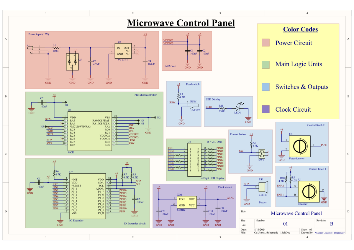
Schematic :
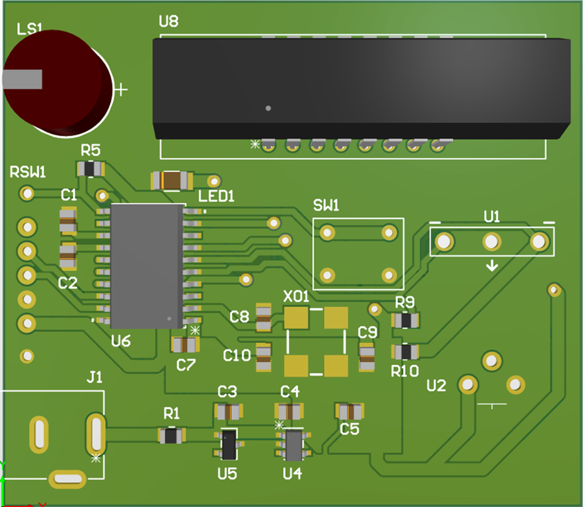
PCB:
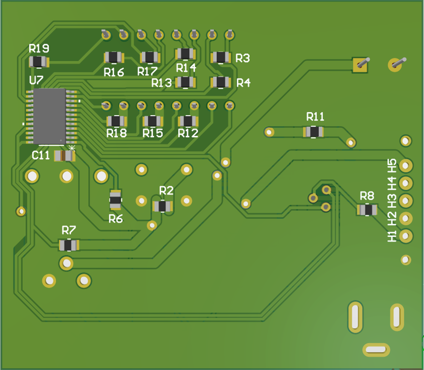
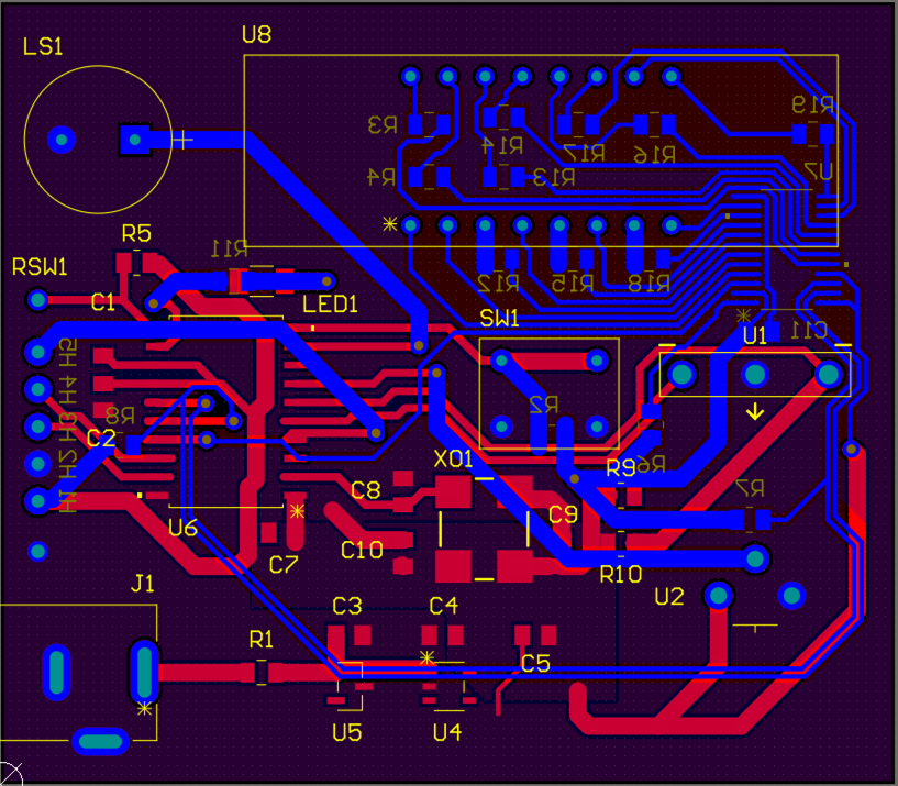
Electronical design
Requirements
To establish the requirements for the Printed Circuit Board (PCB), I first summarized the needed components to match the functions of the studied microwave: - A 4-digit 7-segment displays array - A tactile switch - A rotary encoder - A potentiometer - A Reed switch - An LED - A microcontroller
Furthermore, the PCB will be ordered on JLC PCB website. Each manufacturer has limited manufacturing capabilities, and production prices vary depending on the complexity of the final assembly. Thus, the board will follow JLC PCB’s design recommendations and will be as unexpensive to order as possible, as it is a personal project. The final board has to be 2 layered, with a copper thickness of 1oz on the top and bottom layers. The internal prepreg will be FR-4 with a thickness of 0.4 mm, making a board total thickness of around 0.45 mm.
Components selection
The selection of components is a sensitive step during the design process, as failing to select an appropriate component will lead to modifications of both the circuit schematic(s) and the PCB. That is, if the flaw is found before the production of the PCB. Past this point, undefined behaviors of the circuit may happen (fried components, explosions, or a non-operational board). One will either need to redesign and reorder new boards or perform manual modifications of the traces if available.
In order to make sure all components match with the circuit’s operating parameters; we need a base which defines these requirements.
The centerpiece of such circuit is its microcontroller. I decided to choose the PIC18F15Q20T-ISO microcontroller for this project. I had never used PIC microcontrollers prior to this, which makes it a perfect candidate for discovering this family of Microcontroller Units (MCUs). To select this microcontroller, I relied on the number of available GPIOs, its memory capacity, and the available protocols to communicate with components I will mention later. According to its datasheet, the PIC18F15Q20T-ISO has 16 I/O pins, is I²C/SPI/UART capable, with 11 ADC. It also includes 32KB of flash memory for its program, 2KB of SRAM during runtime, and 256B of EEPROM memory. Using an MCU with more memory than needed will allow for potential heavier updates of the software in the future. The PIC18F15Q20T-ISO operating voltage is 1.8V to 5.5V. Thus, using an LDO with 5V as an output, we can safely power this MCU for multiple applications. From this point, the target operating voltage of any component of the circuit is 5.5V or more.
For better accuracy, I decided to add an external CB3-3C-64M0000 64 MHz oscillator clock to the MCU. This model is 50 ppm, which means that the clock will drift of around 1 minute every 12 days (50’ of drift for 1 000 000’). As the goal of this project is to simulate a microwave and not to actually make one, the board isn’t expected to remain plugged for more than a few hours at most. I chose to take an unprecise clock to cut costs, while still benefiting from a sufficient precision for my needs.
To power the circuit, I chose the PJ-002A power socket as an entry, rated for 24VDC at up to 2.5A. The voltage, assumed to not exceed 12V (although it could safely reach 24VDC), will be converted to 5V by the TPS7B92050DBVR LDO, before being sent to the MCU. To protect the LDO in case of a transient voltage spike, I decided to add a MMBZ16VAT-QR TVS diode of operating voltage up to 13V with an Electrostatic Discharge (ESD) protection reaching up to 30kV.
The TDCR1060M will be the clock display for this PCB. This IC is an interesting one as it uses only 16 pins to manage 4 common cathode 7-segment displays and an active column in the middle. 16 pins are however the total number of pins the MCU can use as GPIO. This is where the PCAL6416APW IO expander comes into play. This I²C IO expander allows the MCU to control the LEDs using only two pins (SDA/SCL). It can also be reset in case of a failure during a communication.
For the switches/indicators, I picked a CMI-9605IC-0580T buzzer, which emits at a fixed frequency of 2.7kHz. The rotary encoder is a 288T232R161A1 2 bits encoder. The datasheet doesn’t specify if the encoder’s outputs are internally pulled-up or down, so I assumed the encoder is open-drain. This means that I had to add pull-up resistors to avoid having floating wires in the circuit. The potentiometer I chose to represent the second control knob is the 2002111655 of the TGN 825 M potentiometers series by Kyocera AVX. This potentiometer has a varying resistance from 100 Ohm up to 1000 kOhm, allowing the MCU’s ADCs to read a rotation angle that the software will convert to a cooking power. Finally, to detect the opening of the door of the oven, I figured one could use a magnet incorporated in its extremity, getting close to a Reed switch, closing a circuit. I used the GP56010-15 switch to do so. This switch has a sensitivity of 15 AT, which is a usual sensitivity value for this application.
The tactile switch is a TS02-66-160-BK-100-LCR-D, and the LED is a 156120VS82500P LED.
Preliminary steps before designs
Before designing the schematic of the circuit and the PCB, a few steps had to be completed. After creating an Altium project for the board, I needed to build a library of all the components I would use for my design. The best place to find 3D models, footprints, and components schematics in my opinion is Ultra Librarian. This way I obtained premade models for the majority of the components and was able to model/integrate the remaining components by myself in Altium Designer. I could also design the missing CAD models, but given the limited utility of doing so, I decided not to. The second preliminary step was setting the design rules to match with JLC PCB’s manufacturing capabilities. This step ensures that the PCB can be produced without complications.
Schematic design
The schematic is split into 12 blocks with distinct colors and functions.
Power input (12V)
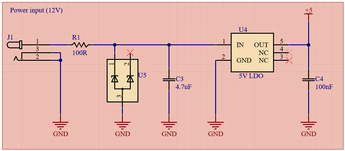 This block is the input circuit. U5 is the TVS diode, U4 is the LDO. R1 limits the current that can flow through U5 in case of an ESD, while C3 and C4 act as decoupling capacitors. Their capacities are given by the datasheet of the LDO.
PIC Microcontroller
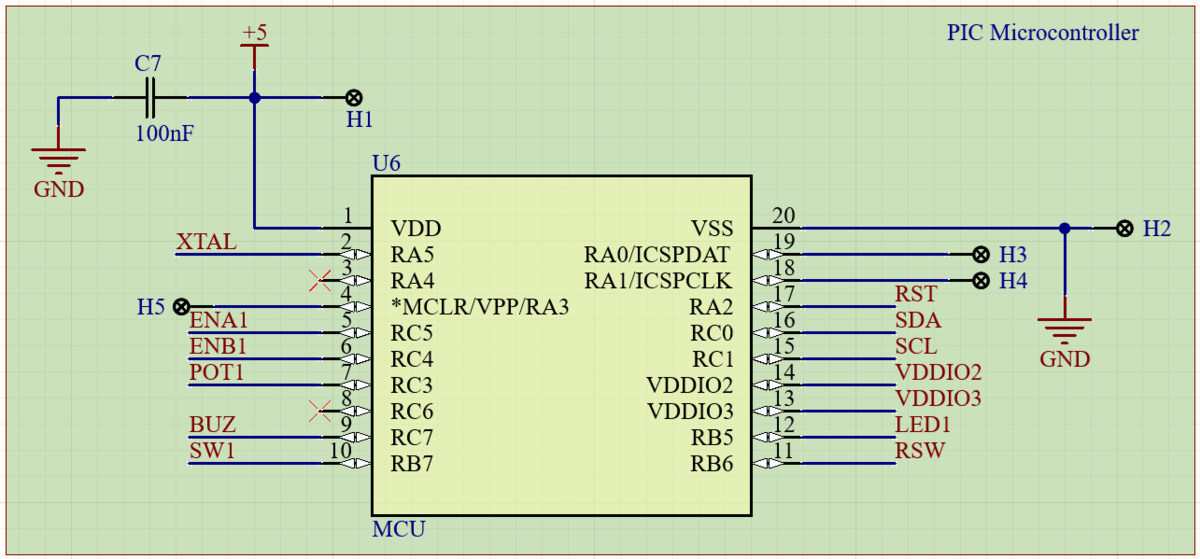
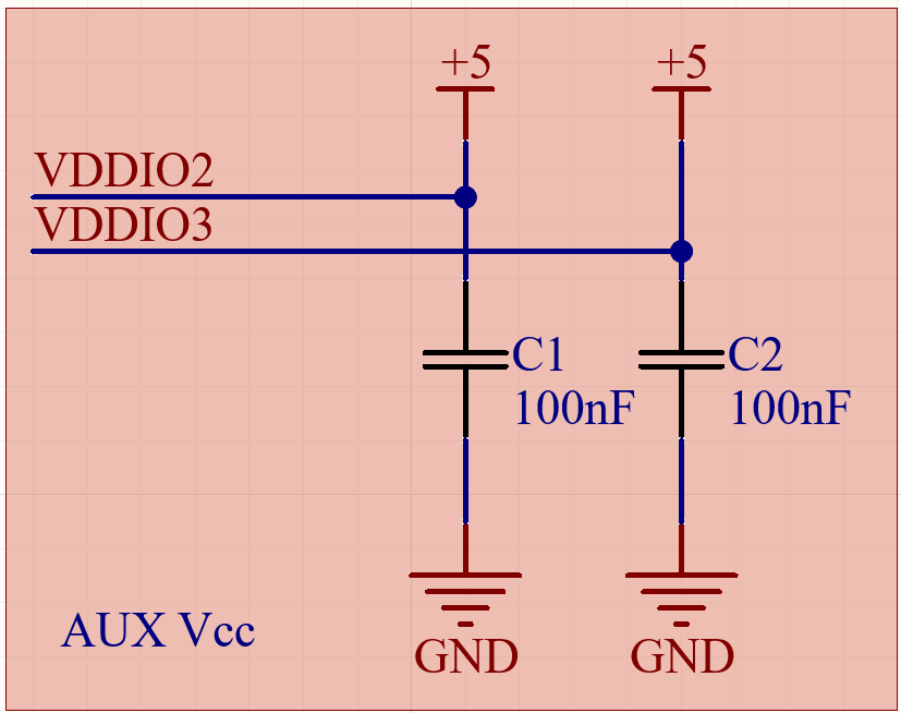 This block contains the MCU and its connections. The pins H1 through H5 are headers that will allow me to flash the MCU with a software. All wires lead to other blocks; they all are located on GPIO pins. The POT1 pin placement had to be carefully done, as it is the connection for the potentiometer. The potentiometer’s value must be read by an ADC of the PIC MCU. According to the PIC’s datasheet, GPIO pins that can be connected to the ADC peripheral are associated with a specific register (ANSEL). The register ANSELC3 is available to use, therefore POT1 was placed on the RC3 pin.
Clock circuit
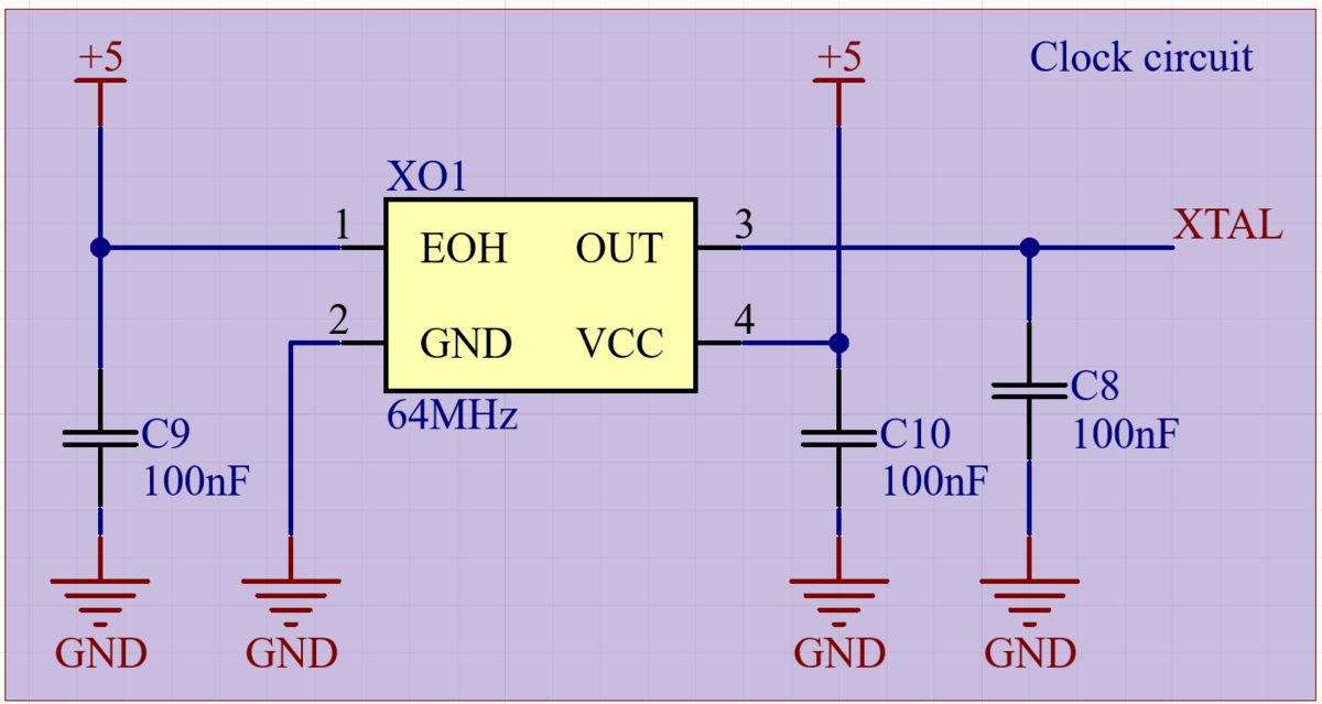 This block is the circuit from which the MCU gets its clock input. The EOH pin of the clock is its activation signal. Since we want the clock to start as soon as the MCU itself starts, I connected it to the 5V rail.
IO Expander circuit
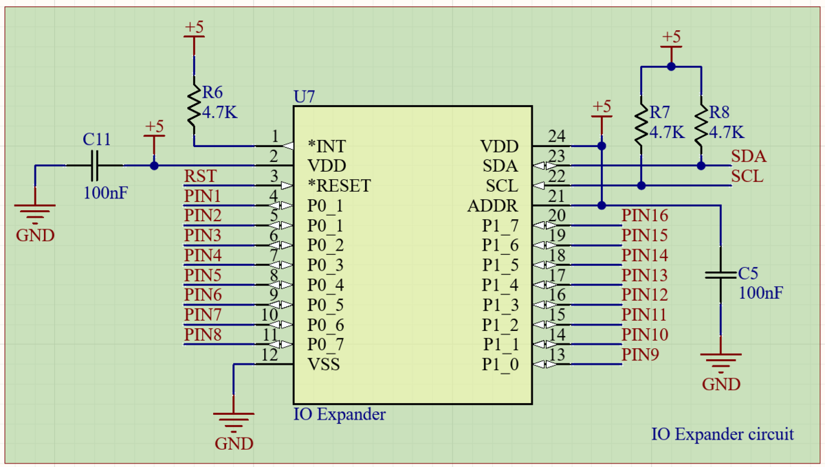 This block is the IO expander circuitry. There are SDA and SCL lines for I²C communication. The IO expander is an open-drain device, so the two lines are pulled up. All the PIN outputs are connected to the LED display.
4 Digit LED Display
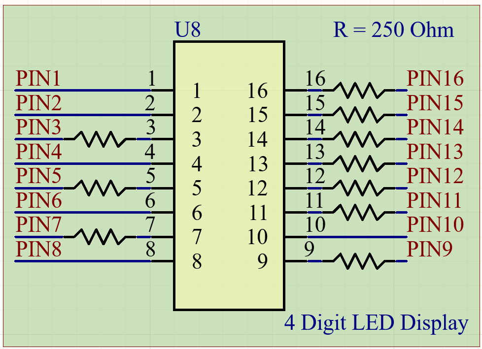 This circuit is the LED Display. The pins 3,5,7,9,11,12,13,14,15,16 are connected to LEDs in parallel. Adding 250 Ohm resistors reduces the current flowing through the diodes while limiting the power dissipated by the resistors. A single resistor with high power dissipation could also have been used in this application.
Control Knobs
These blocks are the implementations of the two control knobs. The first block is the encoder, which is open drain as mentioned before. I added two pull-up resistors to compensate for the floating wires. The datasheet mentions a switch bounce of 5ms at most, which can be corrected by the software. The second control knob is the basic integration of an analog device, with POT1 being the cursor.
Buzzer
The buzzer circuit is the simplest in the board; the impedance of this kind of device is such that no additional resistor is required for it to operate.
Switches
These are the switches blocks. Both of these switches are pulled-up, which means the software must read them as active LOW devices.
LED Display
This is the last block of the schematic. The LED can sustain 20mA continuously, thus a 250 Ohm resistor at 5V is appropriate to reduce its input current.
PCB design
Designing a PCB takes time. The placement of components must be done to allow and simplify the connection of nets on the board. As the board has 2 signal layers, I was able to place components in a way that the interface of the microwave is on one side, while most of the passive components are on the other side. PCB design is an iterative process, the final board was obtained after multiple versions, reducing the number of traces, vias, and overall board size by more than 30% compared to the first design of the board.
Conclusion
In conclusion, the microwave control panel project represents a comprehensive exploration into the design and implementation of an embedded mechatronic system. From the initial motivations driven by a passion for electronics and embedded systems, through the meticulous process of component selection, schematic design, and PCB layout, this project has been both a technical challenge and a valuable learning experience.
By reverse-engineering the control interface of a Samsung MG23F301TAS microwave, I successfully replicated its user interface functionalities without the hazardous high-voltage power electronics. The design choices, such as using the PIC18F15Q20T-ISO microcontroller, the TDCR1060M clock display, and the PCAL6416APW IO expander, reflect a balance between technical requirements, cost-efficiency, and expandability.
The iterative design process emphasized the importance of preliminary research, component compatibility, and careful PCB design, especially when considering manufacturer constraints and design-for-manufacturing principles. Encountering and resolving challenges — from ensuring proper voltage regulation with the TPS7B92050DBVR LDO to integrating a 64 MHz oscillator for MCU timing — strengthened my problem-solving skills and highlighted the need for both precision and adaptability in mechatronic projects.
Ultimately, this project not only solidified my technical expertise but also demonstrated my ability to tackle complex system designs methodically. It serves as a stepping stone for future endeavors in embedded systems and electronics design, equipping me with the confidence and experience to handle even more intricate projects ahead.